Surface treatment technologies are used to clean the surfaces of silicon wafers and glass panels in the electronics industry, especially semiconductor and liquid crystal panel manufacturing.
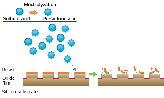
The manufacturing process of products such as semiconductors and liquid crystal panels includes a wet process that involves cleaning the surfaces of semiconductor substrates and liquid crystal glass panels with ultrapure water or chemicals to remove any fine particles, and, previously, large amounts of chemicals were used in this process. As an alternative to this method, surface treatment technologies using functional water are attracting attention. By dissolving specific gases in ultrapure water, it is possible stabilize the substrate surface through oxidation and prevent static electricity, in addition to enhancing the cleaning effect. By using functional water containing dissolved hydrogen gas or ozone gas, it is also possible to significantly reduce the use of chemicals. Furthermore, resins called resists, which are used when forming semiconductor circuits and removed after formation of the circuit, are peeled off using large amounts of chemicals. There is a surface treatment technology using a sulfuric acid electrolysis process which is highly effective for peeling off resists, enabling significant reductions in chemicals compared with previous methods.
Kurita uses these surface treatment technologies to provide high added value devices for semiconductor and liquid crystal manufacturing processes.


